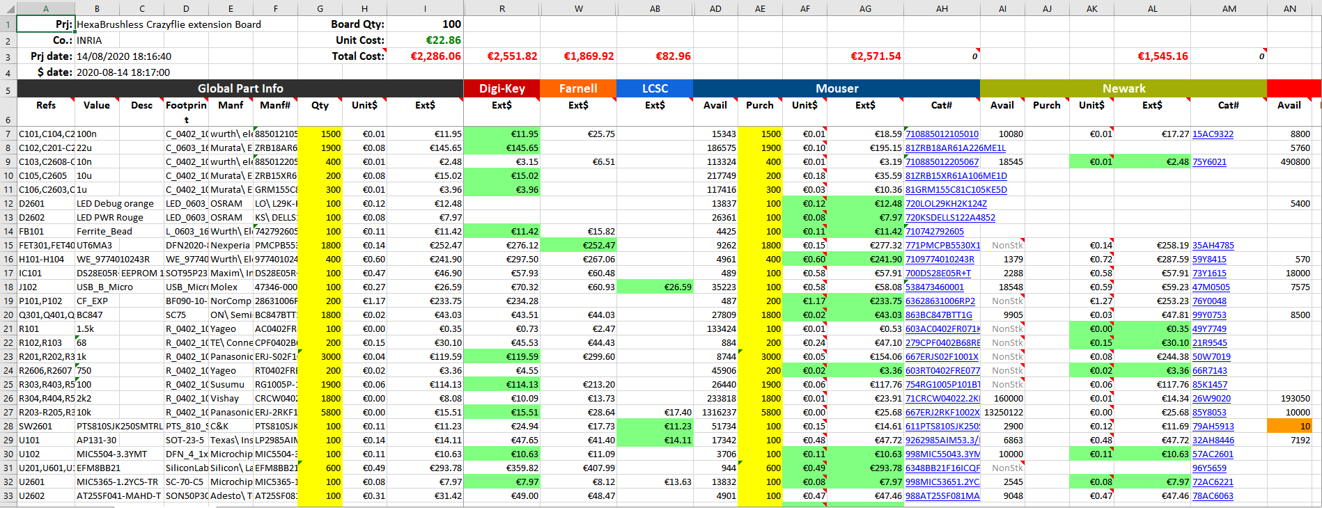
The BOM (Bill Of Material) is a file that regroups all the components information (quantity, manufacturer part number, etc) It is important to do is at the same time the schematics is done, the more late it is done the more tedious it is to do. The more components you have the more complex it get.
In Kicad, the BOM is generated directly as xml, then I use a very good program Kicost to format and get prices of the components from various supplier. It can be a real nightmare to replace components that are not active anymore, that’s why it is important to check early if the component is in stock and is not reaching its end of life soon.
BOM generated with Kicost
Orders
Components
Thanks to the BOM file generated you can order the component from your favorite supplier.
PCB
After the PCB layout done of Kicad, Gerber’s file need to be generated. Theses standard files allow manufacturers to print your PCBs.
PCBs can also be manufactured in-house by using milling technique. It has the advantage to be ready to use in half a day. However it is limited to double sided PCB and the quality is quite pretty bad in comparison to professional chemical etching technique. (See post about PCB milling.)
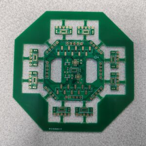
Preparation
Once all the components and the PCB delivered, it is important to check if you have all the components and the correct quantities. For that I like to use a barcode scanner to auto search and check the components.
I use the Kicad addon InteractiveHtmlBom to keep track of all the components.
Manual Pick and Place setup
Solder paste
To apply solder paste on the board, I usually maintain the board I’m working on with other taped PCBs with the same thickness. Then I place the stencil and tape on the side to be able to open it and place other PCB if I need to.
Then I apply some paste on the stencil and spread it with a spatula.
PCB with solder paste
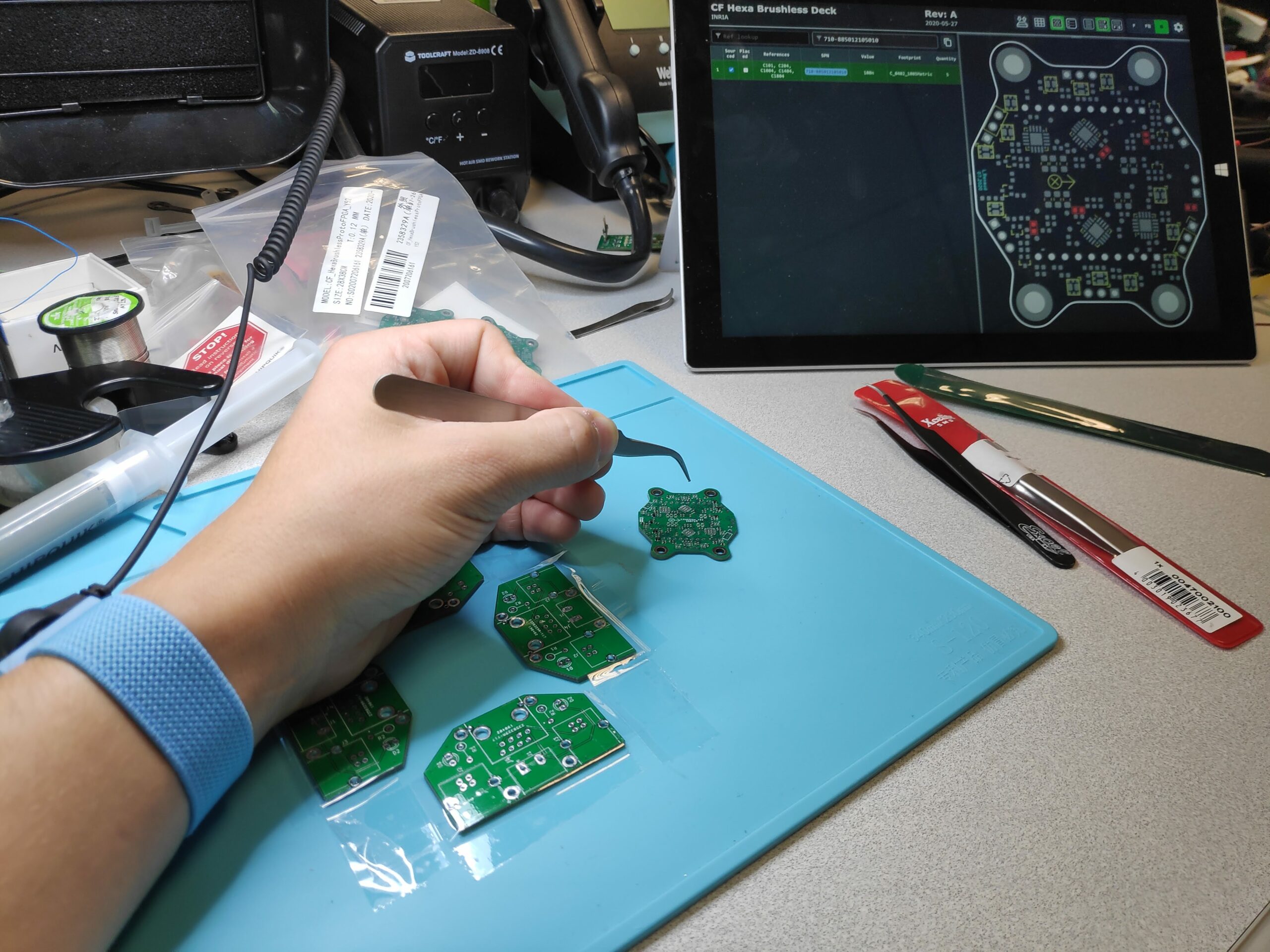
Manual Pick and Place (PnP)
Manual Pick and Place is the main and more tedious step. A lot of patience, good eyes and a steady hand are required. I usually start by placing the smaller components and finish by the bigger ones to avoid being constrained.
To check the location of the component and because I don’t generally use reference on the silkscreen (because of the space it takes) I always use the HTMLInteractiveBom software tool.It highlights the location of the components and allow to not forget any.
PnP
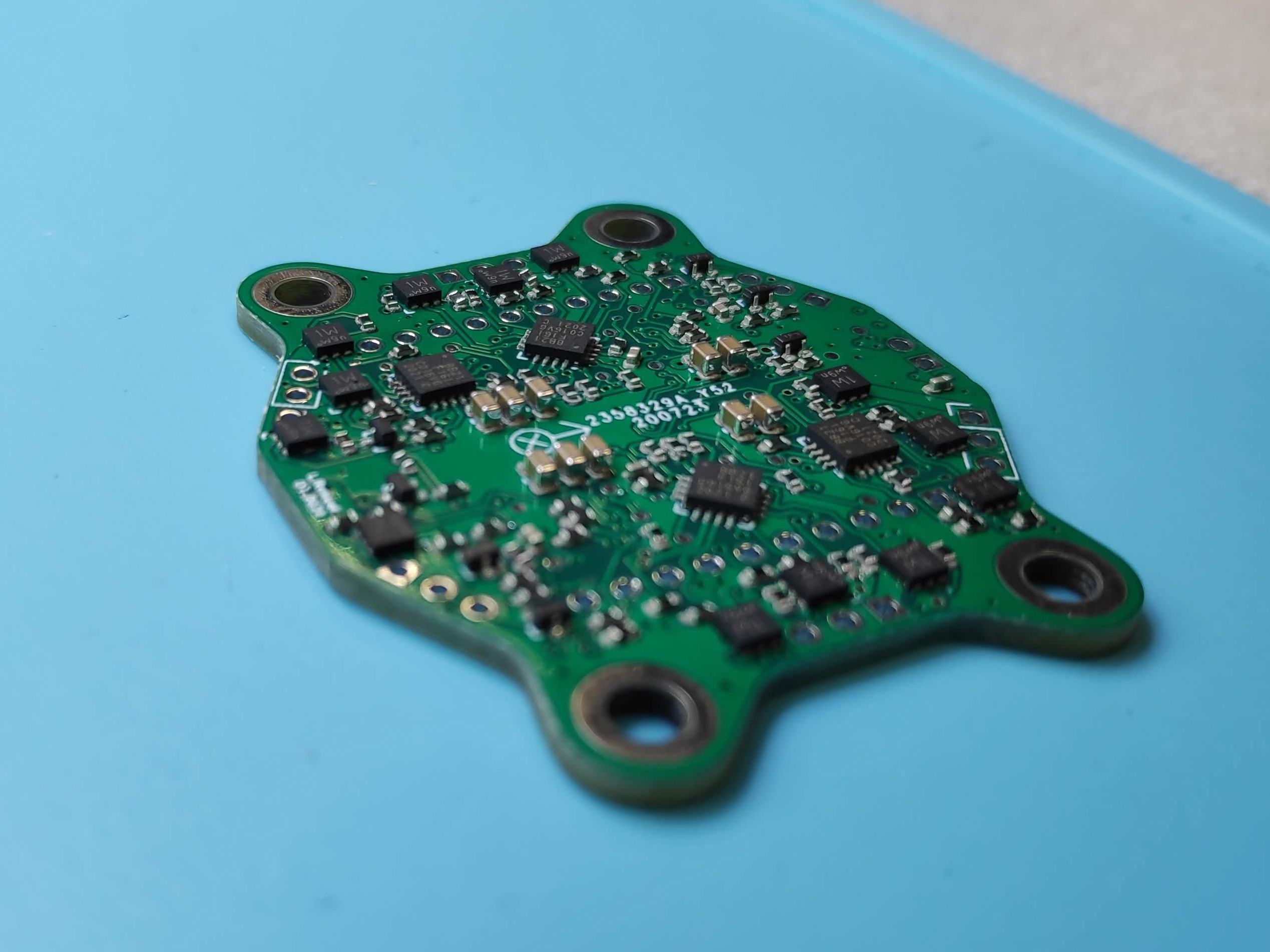
Populated board
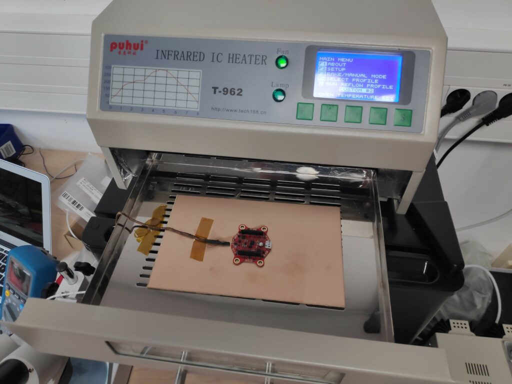
Soldering
To solder the components I usually use a airflow solder iron. It allows me to visually control the soldering of all component pads, and avoid overheating of components like connectors that tends to melt in a reflow oven.
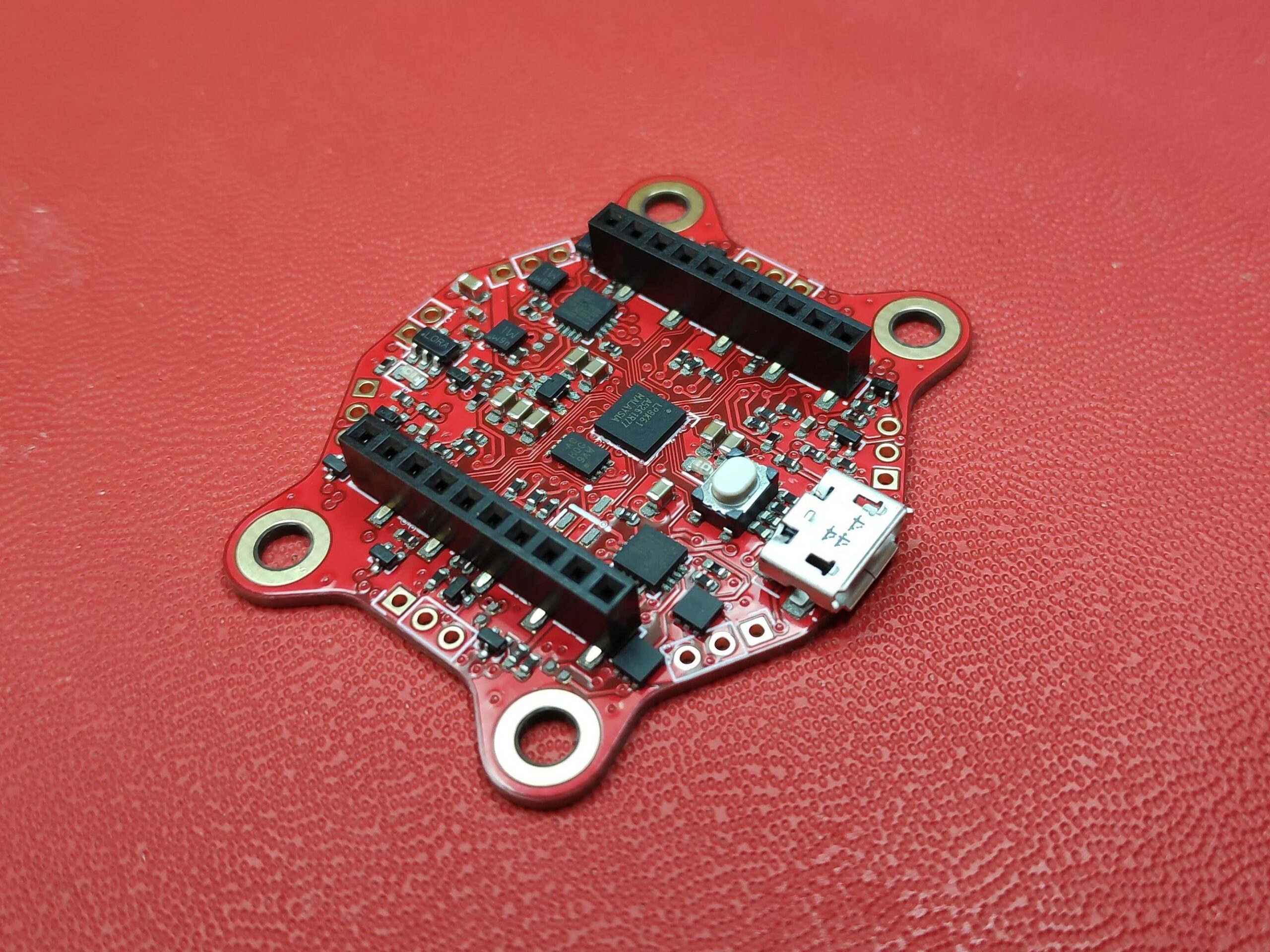
Inspection
After the reflow process, we need to inspect the board and check all the pads and if all the components are well soldered. Binocular is a great help for that step.